The battery is built.... Now for

D

Deleted member 4366

Guest
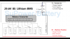
You'd get 30 amps and nearly 15Ah out of 13S4P Panasonic/Samsung GA cells, which would be about 1/3 the weight, then you need to find a way/place to mount it. Maybe get one of the empty 09 cases.
 

Danidl

Esteemed Pedelecer
Sep 29, 2016
8,610
12,256
73
Ireland
No, that's not true. the only thing that matters is the voltage. current can only flow between them when there's a voltage difference. I've run a12s LiFepO4 in parallel with a 10S Li-ion for 6 months with no detrimental effects, and that was charging only through one of them, though in theory, that can give balance problems, which can cause consequences.

Am I reading you correctly? Say one battery is at 41 V and the other at 40 then there is 1 volt difference . If both are paralled current will flow between them to attempt to equalise. The resistance of these battery packs is in the milliohm range, so this current could be in the 100s of amp range, limited only by the accidental resistance of the connecting wires, connectors and switches
 

Nealh

Esteemed Pedelecer
Aug 7, 2014
20,126
8,226
60
West Sx RH
Looking at a couple of pics from when I opened my 09 battery for cell checking.
The N -- is a thinner black wire and AFAICT picks up the ground from the batt pack for a switch connection on the bms, the N + is red and goes to the swtich.
 
Last edited:
D

Deleted member 4366

Guest
Am I reading you correctly? Say one battery is at 41 V and the other at 40 then there is 1 volt difference . If both are paralled current will flow between them to attempt to equalise. The resistance of these battery packs is in the milliohm range, so this current could be in the 100s of amp range, limited only by the accidental resistance of the connecting wires, connectors and switches
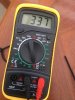
That's it, but it's not as severe as that implies with only 1v difference. Obviously, the closer they are too the same voltage, the better. After the initial levelling, they hold each other at the same voltage.
 

Low

Pedelecer
Dec 5, 2016
142
42
45
England norfolk
Looking at a couple of pics from when I opened my 09 battery for cell checking.
The N -- is a thinner black wire and AFAICT picks up the ground from the batt pack for a switch connection on the bms, the N + is red and goes to the swtich.
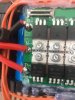
Interesting, i there isnt a n+ on the board do you thhink it can be ignored the is just B- N- P- on this bms

Perhaps its racist?
 

awol

Esteemed Pedelecer
Sep 4, 2013
1,216
374
This video discussed wiring the BMS


Low

Pedelecer
Dec 5, 2016
142
42
45
England norfolk
Ty... Just struggle with that screaming mad guy :)

Il turn the volume down :)

Was a different guy... Great Vid

His bms didnt have BNP he had BCP

I know im being dumb! Is the N the same as the C or does my P do the the C as well and i ignore N

Answers in the style of child talk would be much appreciated!
 

Nealh

Esteemed Pedelecer
Aug 7, 2014
20,126
8,226
60
West Sx RH
Can't be 100% but the N -- could be bms to charger connection if there isn't a C --.
 
D

Deleted member 4366

Guest
The BMSs are normally marked B- (negative from cell pack); P- (negative output); C- (negative charger). In most cases the charger positive and output wires go straight to the cell-pack, though some BMSs need a separate positive connection, marked B+. Occasionally the B+ pas is only used as a terminal to join B+, C+ and P+. I never heard of a N+ or N- connection.

here's a schematic:

 
D

Deleted member 4366

Guest
I've just looked at the first photo of your BMS. There doesn't appear to be a separate charging mosfet, so all 8 mosfets are switching on/off the power for charging and discharge together. That would mean that C- and P- must be joined on the PCB. you can use a meter on beep to test that. If it beeps between N- and P-, then N- is C-
 
D

Deleted member 4366

Guest
Lets start with a convention for the mosfets. You look at one with the black face towards you and the legs downwards. The left leg is the one that provides the signal to switch and the other two legs are the switch.

In your last photo, B- (normally pack negative) goes through the shunts and then to the 4 right legs in parallel. The backs of the mosfets are common with the middle leg and are all soldered to the PCB and goes to N-, so they're switching between N- and B-.

The bottom bank have their right legs connected to P- and their middle legs connected to N-, so they're switching between P- and N-. As the middles are joined, that means that P- is joined to B- when all mosfets are switched on, which is conventional and the markings are conventional. N- will switch on at the same time as P-, so logic says that it must be the charger negative connection.

I've just been looking at another BMS that has a similar back-to-back arrangement of the mosfets. it has no middle connection point (N-). Instead, both the charger and discharge wires are joined together and go to the P- pad. In practice, it makes no difference. Basically, when the mosfets all switch on together N-, P- and B- are all joined together; however each bank has separate signal connections, so I guess that each bank could be switched independently. That means that the top bank can allow charging while the lower bank is switched off. Normally you'd want to switch off charging but allow discharging too, which can't happen with that arrangement.

One last question that might solve it. Do all the mosfets have the same markings?
 

Low

Pedelecer
Dec 5, 2016
142
42
45
England norfolk
You know your stuff, it will take me a while to digest what you wrote..

All the markings are the same.

Just found this, litterally all iv found all day.

Il have s read of your last post now, ty v much for your patience.image.png
 
D

Deleted member 4366

Guest
That makes it the same as my one then. Just ignore the N- and leave it disconnected. Whichever bank goes off, both charging and discharging are interrupted. My guess is that one bank goes off when a cell voltage is too high and the other goes off when a cell is too low.

in your last photo, it looks like the left bank gets switched on by the transistors in the group Q13, Q15, Q9, Q10 and Q14 and the right bank by Q11 and Q12
 
  • Like
Reactions: robdon

Advertisers